Trollectronics™ Trollbook™®©
The Motorola 68k is a wonderful series processors. 32 bit, nice cisc architecture, many registers, old and crummy enough to be friendly for hobby level hacking, yet fast enough to pull off some cool stunts (looking at you, amiga). Obviously Slaeshjag and I needed another project. Obviously this project had to be a portable MC68k based computer.
First Revision
The first brainstorming started in late 2014. We decided to use a 25 MHz MC68030 processor and a larger Xilinx CPLD for the glue logic/peripheral controller. The system would be a mixed 5V and 3.3V system, since the SDRAM chips we planned on using were 3.3V only. We ordered a CPU and CPLD from Ebay and started work on the schematic and PCB layout in November 2014. Work continued during early 2015. An emulator was developed so we could develop an operating system for our new computer.
Second Revision
In autumn 2015, the project had somewhat stalled. The board layout needed a rework and motivation was somewhat lacking. This is the time when you find a better processor for cheap on Ebay and decide to redo everything from scratch!
Yes. That happened. We found an MC6040V that could do 33 MHz, The 'V' means that the CPU will run on a 3.3V supply. Nice. We also found a couple of cheap Altera Flex10k FPGA:s from an electronics import and surplus store. These are 3.3V devices and will replace the Xilinx CPLD in the design. We decided to go for a 4 layer PCB, 10×10 cm large for the CPU, FPGA, RAM and ROM. The plan is to have this board connected to another board, 16×10 cm large, with the keyboard and some serial peripherals. A battery will be wedged in between the boards and a 7" LCD mounted like a laptop screen and closed like a clamshell. We immediately started redesigning the board. With four layers and only one supply voltage, everything was much easier to lay out.
Since we had borrowed an Altera DE2 FPGA devboard from school for a course, I figured that I might as well use it to play around with generating VGA timings, something that would come in handy later when our 7" LCD arrived. I then managed to set up a small test circuit for the LCD using a tiny Xilinx XC9572 CPLD to drive the sync signals and a couple of colours.
Update 2016-03-22
We have now ordered and received the boards! First thing to do was of course to solder the FPGA and LCD connector and try out the VGA timing code on the actual hardware. I decided to solder most of the other components, including the CPU and the SRAM, but leaving the DRAM out for now. The board is looking really nice.
Update 2016-04-07
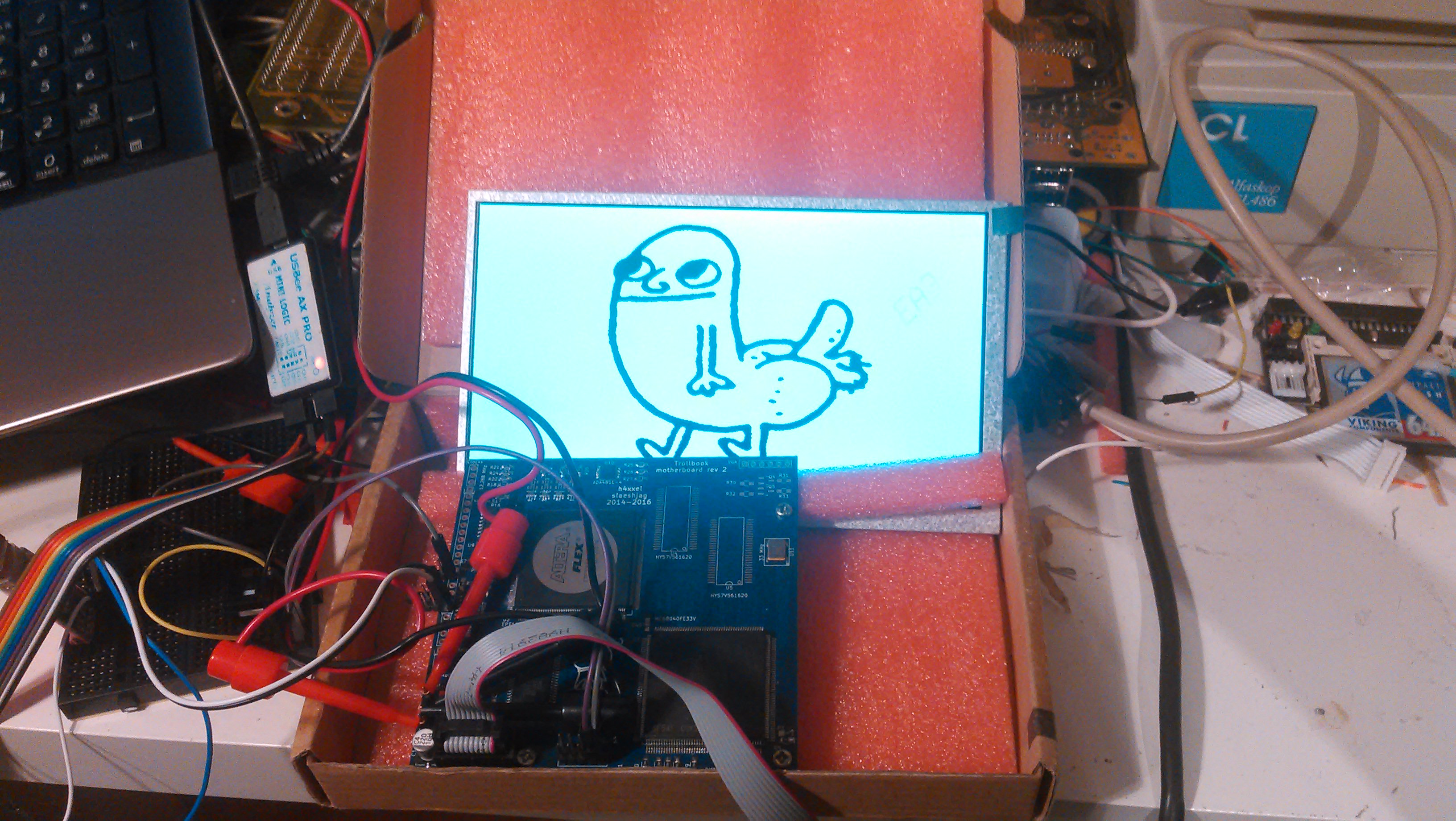
The CPU is now running actual code. The pattern on the screen is actually genereted by the CPU, writing to the framebuffer. Proper adress decoding is however not in place yet. All reads are fetched from a boot ROM internal to the FPGA and all writes are sent to the frame buffer RAM. It is however great to see this thing actually working. Reaching this point required lots of cursing, staring at the simulator and shouting that this should indeed work. Slaeshjag pointed out that I should probably check the soldering of the board, especially the adress lines... Voila.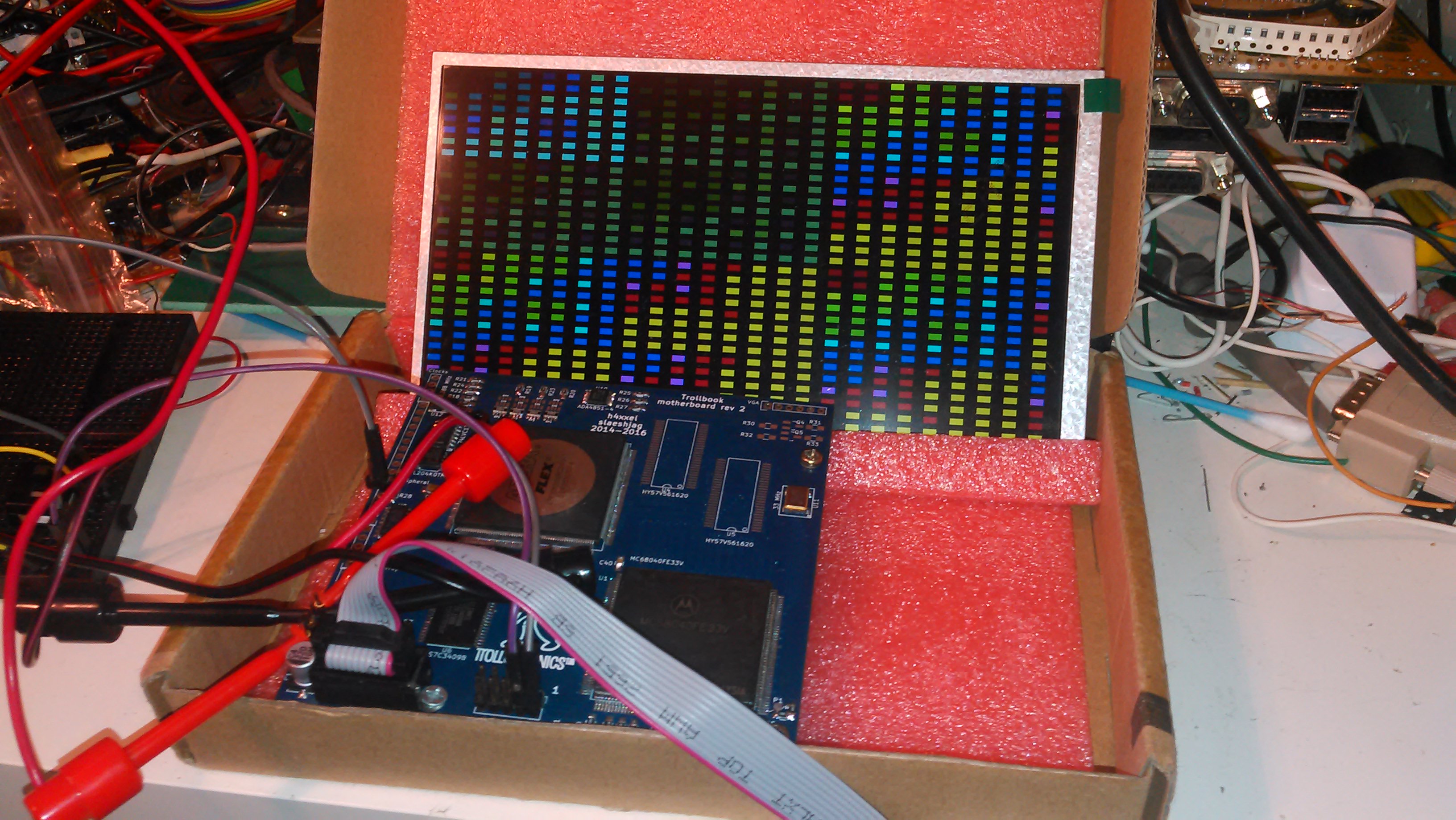
Update 2016-04-11
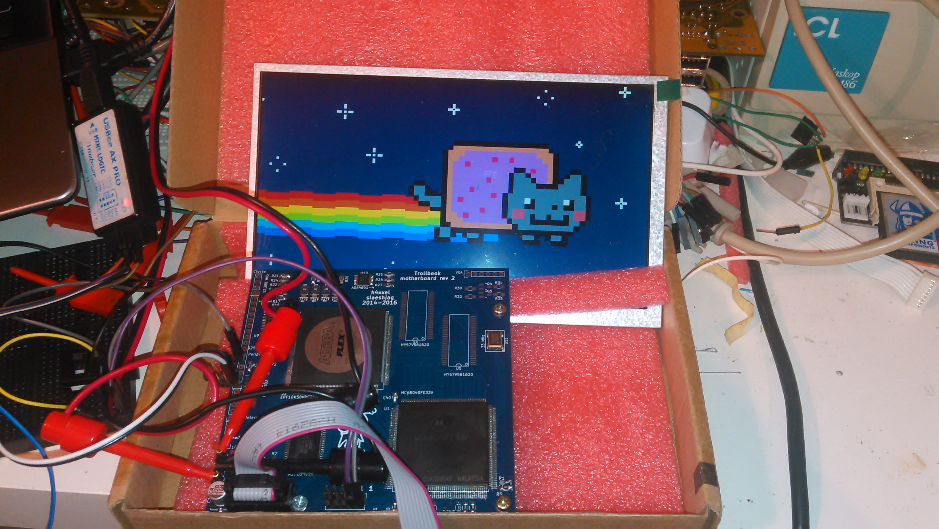
We have now gotten the serial port to work and we have some proper address decoding and bus multiplexing in place. This means we can send pictures over the serial line! At first we had som issues with the colour palette and the speed of the serial line. It was however fixed and we can now send colour images at 115200 baud. Amazing.
Update 2016-12-09
Long time since the latest update, but we have not abandoned the project! On the contrary, rather. During the beginning of the autumn we started working on an SPI controller in the FPGA and soon managed to talk to an SD card and later also the SPI ROM. We made a temporary power supply board that could supply 3.3 V for the board and 23 V for the LCD backlight without the need for a bulky multi-voltage bench power supply. We also wrote lots of BIOS code and implemented a menu system and SD card file browser. I wanted to make a progress update on this page during mid-autumnbut kind of forgot about it.
We also soldered the SDRAM and started writing VHDL code to interface it. This is where we ran into problems and progress stalled somewhat. During late november/early december we decided to make a small SDRAM test board with only an SDRAM chip and a small Xilinx CPLD on it, and all the address, data and control signals easily accessable on a pin header. This way we could hook up the logic analyzer and look at what was actually going on.
We found out that it was a timing issue. In the SDRAM datasheet, it looks like outputs are changed on the falling edge on the clock and inputs are sampled on the rising edge. This turned out not to be the case, and could actually also be verified by looking very closely in the datasheet. All signals are changed and sampled on the rising edge. The reason why it looked different in the datasheet was because the propagation delay of the output was drawn in all the timing charts. At 133 MHz, the delay would have caused the signals to change approximately at the same time as the clock falls, however we only run at 33 MHz. We managed to fix the problem by inverting the clock phase relationship between the cpu and sdram and some minor changes to the VHDL. Now we have 64 MB of ram to play with, seems like it is soon time to get an OS running on this thing.
... So we also started working on getting the MMU (memory management unit) working. The MMU of the 68040 is very different from the MMU in the 68030, so we had to rewrite all of our old MMU code in trollos. We got the MMU working within a couple of days however and could run a small demo program from a virtual address space. We decided to make a video of this demo.
We also started working on the emulator again, updating all the peripheral controllers for the new design, as well as updating the CPU core to the 68040.